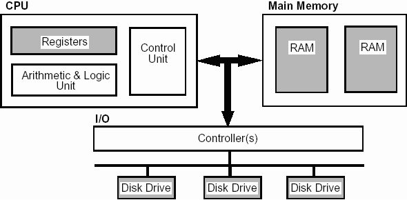
Memory
Memories hold one or more bits of information:
The contents of a memory remain unchanged unless overwritten with a new bit pattern. For some memories the contents are "lost" when power to the memory is turned off.
Computers employ many different types of memory (semi-conductor memory, magnetic disks and tapes, CD-ROMs etc.) to hold data and programs. Each type of memory has its own characteristics and uses.
Register Memory
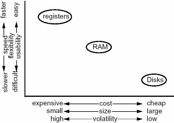
Registers are memories located within the Central Processing Unit (CPU). They are few in number (there are rarely more than 64 registers) and also small in size, typically a register is less than 64 bits in size.
The contents of a register can be ôreadö or ôwrittenö very quickly however, often an order of magnitude faster than main memory and several orders of magnitude faster than disk memory.
Different kinds of register are found within the CPU. General Purpose Registers are available for general use by the programmer. Unless the context implies otherwise weĺll use the term "Register" to refer to a General Purpose Register within the CPU. Most modern CPUĺs have between 16 and 64 General Purpose Registers. Special Purpose Registers have special uses and are either nonprogrammable and internal to the CPU or accessed with special instructions by the programmer.
Examples of such registers include:
Although Register Size (the size of the Register bit-group) tends to vary according to register type, the Word Size of an Architecture is often (but not always!) defined by the Size of the General Purpose Registers.
In contrast to Main memory and disk memory, registers are ôaddressedö directly by specific instructions or by encoding a register number within a computer instruction. At the programming (assembly) language level of the CPU, registers are normally specified with special identifiers (e.g. R0, R1, R7, SP, PC)
A final point, the contents of a register are lost if power to the CPU is turned off, so registers are unsuitable for holding long-term information or information that is needed for retention after a power-shutdown or failure. Registers are however, the fastest memories, and if exploited can result in programs that execute very quickly.
Main Memory (RAM)
If we were to sum all the bits of all registers within CPU, the total amount of memory probably would not exceed 5,000 bits. Most computational tasks undertaken by a computer require a lot more memory. Main memory is the next fastest memory within a Computer and is much larger in size.
Typical main memory capacities for different kinds of computers are:
| Personal Computer | 256MB |
| Fileserver | 4GB |
| Database Mainframe | 32GB |
Computer Architectures also impose an architectural constraint on the maximum allowable RAM. This constraint is normally equal to 2WordSize memory locations
RAM (Random Access Memory) is the most common form of Main Memory. RAM is normally located on the motherboard and so is typically less than 12 inches from the CPU. ROM (Read Only Memory) is like RAM except that its contents cannot be overwritten. ROM memory is often used to store the ôbootö or start-up program that a computer executes when powered on.
Although slower than register memory, the contents of any location in RAM can still be ôreadö or ôwrittenö very quickly. The time to read or write is referred to as the access time and is the same for all RAM locations.
In contrast to register memory, RAM is used to hold both program code (instructions) and data (numbers, strings etc). Programs that are running are normally ôloadedö into RAM from a disk prior to execution by the CPU.
Locations in RAM are identified by an addressing scheme e.g. numbering the bytes in RAM from 0 onwards. The contents of RAM are lost if the power is turned off.
Disk Memory
Disk memory is used to hold programs and data over the longer term. The contents of a disk are NOT lost if the power is turned off. Disk capacities range from 2GB to over 40 GB (40 × 109). Disks are much slower than Register and Main memory, the access-time to data on disk is typically between 5 and 15 milliseconds (5 × 10⁻³ sec), although disks can typically transfer hundreds or thousands of bytes in one go.
Disks can be housed internally within a Computer ôboxö or externally. There are also many kinds of Disk unit, e.g: Magnetic Hard Disks, Floppy Disks (V. Slow), Magneto-Optical CD Roms/Disks, DVDs.
Disk locations are identified by special disk addressing schemes (e.g. track and sector numbers).
Summary of Characteristics
Main Memory Organisation
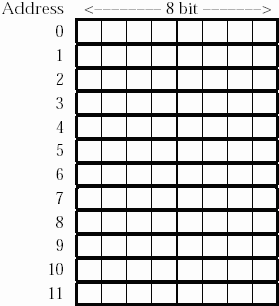
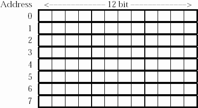
We can imagine Main Memory to be organised as a matrix of bits. Each row represents a memory location, typically this is equal to the word size of the architecture, although it can be a word multiple (e.g. 2xWordsize) or a partial word (e.g. half the wordsize). For simplicity we will assume that data within Main memory can only be read or written a single row (memory location) at a time.
For a 96-bit memory we could organise the memory as 12 × 8 bits, or 8 × 12 bits or 6 × 16 bits, or even as 96 × 1 bits or 1 × 96 bits. Each row also has a natural number Address which is used for selecting the row:
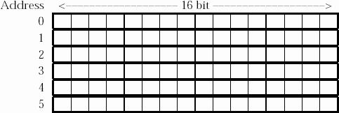
Byte Addressing
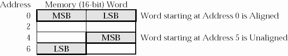
Main-memories generally store and recall rows, which are multi-byte in length (e.g. 16-bit word = 2 bytes, 32-bit word = 4 bytes). Most architectures however, make Main Memory byte-addressable rather than word addressable. In such architectures the CPU and/or the Main Memory hardware is capable of reading/writing any individual byte. Here is an example of a Main memory with 16-bit memory locations. Note how the memory locations (rows) have even addresses.

Byte Ordering
The bytes within a multi-byte data item can be numbered from Left-to-Right (Big-Endian) or from Right-to-Left (Little-Endian). In the following example, table cells represent bytes, and the cell numbers indicate the address of that byte in Main Memory.
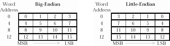
In Big-Endian systems the most significant byte of a multi-byte data item has the lowest address, while the least significant byte has the highest address.
In Little-Endian systems, the least significant byte of a multi-byte data item has the lowest address, while the most significant byte has the highest address. Note: an N-character string value is not treated as one large multi-byte value, but rather as N single character values, i.e. the first character of the string always has the lowest address, the last character has the highest address. This is true for both big-endian and little-endian.
Example: Show the contents of memory at word address 24 if that word holds the number given by 122E 5F01H in both the big-endian and the little-endian schemes?
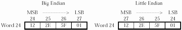
Note: By convention, we order the bytes within a memory word left-to-right for big-endian and right-to-left for little-endian.
Example: Show the contents of main memory from word address 24 if those words hold the text JIM SMITH.
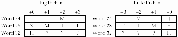
The bytes labelled with ? are unknown. They could hold important data, or they could be donĺt care bytes ľ the interpretation is left up to the programmer.
Unfortunately computer systems, in use today are split between those that are big-endian, and those that are little-endian. This leads to problems when a big-endian computer wants to transfer data to a little-endian computer. Some recent architectures (e.g. PowerPC) allow the endian-ness of the architecture to be switched programmatically.
Word Alignment
Although main-memories are generally organised as byte-addressed rows of words and accessed a row at a time, some architectures, allow the CPU to access any word-sized bit-group regardless of its byte address. We say that accesses that begin on a memory word boundary are aligned accesses while accesses that do not begin on word boundaries are unaligned accesses.
Reading an unaligned word from RAM requires
Writing an unaligned word is even more complex and SLOWER. For this reason some architectures prohibit unaligned word accesses. e.g. On the 68000 architecture, words must not be accessed starting from an odd-address (e.g. 1, 3, 5, 7 etc). Some architectures extend this principle to multi-word accesses. e.g. on the SPARC architecture, 64-bit data items must have a byte address that is a multiple of 8.
RAM Integrated Circuits (Chips)
So far, we have looked at the logical organisation of Main Memory. Physically RAM chips can be organised in a variety of ways also. Here are 3 methods for forming a 256x8 bit main memory.
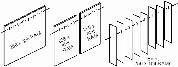
In the first case, Main memory is built with a single RAM chip. In the second we use two RAM chips, one gives us the most significant 4 bits, the other, the least significant 4 bits. In the third we use 8 RAM chips, each chip gives us 1 bit - to read an 8 bit memory word, we would have to access all 8 RAM chips simultaneously and concatenate the bits.
Memory Banks
Main memories are normally bigger than the size of a single RAM chip. Therefore to access a memory word the memory hardware has to read a row in several RAM chips simultaneously and then concatenate the returned results from each RAM chip.
The RAM chips that make up a main-memory system, are normally grouped into banks that are one memory word wide:
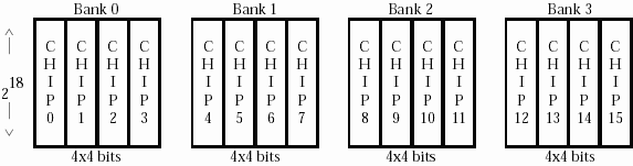
Example: Given Main Memory = 1M × 16 bit (word addressable),
RAM chips = 256K × 4 bit
BANK size = RAM chips per memory word = Width of Memory Word / Width of RAM Chip = 16/4 = 4
18 bits are required to address a RAM chip (since 256K = 218 = Length of RAM Chip)
A 1M × 16 bit word-addressed memory requires 20 address bits (since 1M = 220).
Therefore 2 bits (20−18) are needed to select a bank.
The Total number of RAM Chips = (1M × 16) / (256K × 4) = 16
Total number of BANKS = Total number of RAM chips / BANK size = 16/4 = 4
Interleaved Memory
When memory consists of several banks, some address bits will select the bank, and the remaining bits will select a row within the selected bank.
If the bank selection bits are the least significant bits of the memory address the resulting memory is referred to as low-order interleaved.
If the bank selection bits are the most significant bits of the memory address the resulting memory is referred to as high-order interleaved.
Interleaved memory can yield performance advantages if more than one bank can be read/written at a time:-
This is an advantage for a single multi-word access of sequential data such as program instructions, or elements in an array of data.
This is an advantage if the CPU can access rows in one bank while at the same time an I/O device (hard disk, etc.) can access different rows in another bank.
Example: Main Memory = 1M × 8bits, RAM chips = 256K × 4bit.
For this memory we require 4 × 2 = 8 RAM chips.
Each chip requires 18 address bits (ie. 218 = 256K).
And 1M × 8 bits requires 20 address bits (ie. 220 = 1M )
last updated: 2-Nov-04 Ian Harries <ih@doc.ic.ac.uk>