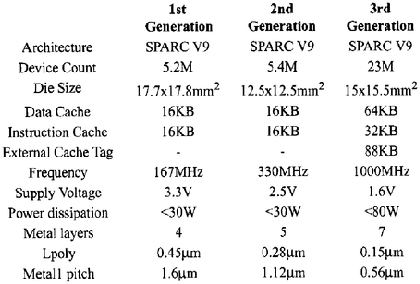
The UltraSPARC-III processor from Sun is the third processor to implement the 64-bit SPARC V9 compliant architecture, [1,2,3] it is the newest in the UltraSPARC generation of processors. The design goals were based on three important factors : scalability, compatibility and performance. Figure 1 shows the comparison between the three generations of SPARC processors.
The design permits high scalability of to build systems consisting of
thousands of UltraSPARC-III processors. The on-chip memory system and the
bus interface were designed to be able to handle systems built using one
to thousands of UltraSPARC-III processors. There are more than 10,000
third-party applications available for SPARC processors, hence binary level
compatibility is an essential goal of any new SPARC processor. The
goal was to try and improve application performance without having
to recompile the application. This improvement in performance must
be application independent - it must apply to all applications and not
to only those which are a good match for the architecture. Also, this design
ensures compatibility with all existing SPARC applications and the Solaris
operating system.
High performance was achieved using a multi prong approach. Recent research
focussed on designing ways to extract more instruction-level parallelism
from programs. The disadvantage was that the speedup varies
greatly across different programs. The reason for this was
that ILP techniques varied greatly between programs, as many programs
use algorithms whose data dependency forces the instructions to be executed
serially. This led to the belief that scaling bandwidth (ILP) alone cannot
improve performance for all programs. The focus was then to scale both
bandwidth and execution latency, ![]() to increase the bandwidth
and reduce the execution latency. Compared to the previous generation, the
clock rate is increased by 150%, and the instruction parallelism is
improved by 15% [2]. Test and debug capabilities are also
included in UltraSPARC-III which has an IEEE compliant 1149.1 test access
port (TAP) and controller [7].
to increase the bandwidth
and reduce the execution latency. Compared to the previous generation, the
clock rate is increased by 150%, and the instruction parallelism is
improved by 15% [2]. Test and debug capabilities are also
included in UltraSPARC-III which has an IEEE compliant 1149.1 test access
port (TAP) and controller [7].
The rest of the paper is organized as follows. Section II gives a detailed description about the architecture of the processor. Section III talks about the Visual Instruction Set, an extension to the SPARC V9 instruction set, which provides instructions that greatly enhance the multimedia and image processing capabilities of the SPARC processors, and Section IV talks about the test and debug capabilities built into UltraSPARC-III. Section V concludes the paper.